CMOS Image Sensor and Image Compression
Guo, Yikun Gao, Shengze Mo, Xunjun Luo, Jingxiong Wan, Xingyu
1. Introduction
This document focuses on the design of an image sensor with image compression capability. It is implemented in 0.35 um CMOS technology with 64*64 pixel array. It uses a single-slope ADC architecture. The row decoder is used to select rows of pixel array. Column ADC compares a ramp signal with pixel signal and converts the latter to digital representation a row at a time. The digital core compresses the digital signal. In addition, a control block is designed to coordinate the timing of the whole chip. Detailed I/O and chip dimension are shown in the floorplan in Figure 1. The schematic and the layout for the entire chip is shown in Figure 28 and 29.
2. Specification
The digital core uses standard 1.2V supply while the analog circuitry uses 1.8V supply to accommodate 0.5-1.5V pixel signal. The clk of digital core is 10MHz with Vp-to-p = 1.2V. The clk of comparator is 25MHz with Vp-to-p=1.8V. The ADC comparison time is 10.6us. The column pitch of the pixel array is 15um. And the ADC resolution is 8-bits.
3. Block Design
Analog
part
3.1 Row decoder
A 6-bits row decoder is used here to select 1 out of 64 rows. A 7-stage decoder
is designed as figure 2. The size of the first stage inverter is sized to be easily
driven by digital circuitry, while the last stage is sized to drive the
capacitance of 64 pixel arrays. Figure 3-5 Shows layout and 6-7 Shows sizing
and simulation results.
3.2 Single-Slope ADC
3.2.1 Ramp generator
It is implemented as an RC integrator. The op-amp and the switch are implemented on-chip. Since one ramp generator is shared for all column ADCs, off-chip precision resistor and capacitor are used for higher accuracy. And a 1pF capacitor is placed at the output to suppress the kickback and the effect of charge injection. Figure 8-9 display the schematics while Figure 10 is the layout of ramp generator.
3.2.2 Column ADC
The column circuit takes the pixel signal and ramp signal as inputs, and produce a digital enable signal controlling a counter. The schematic for the column circuit is shown in Figure 11. It mainly consists of a pre-amplifier, a latch comparator [3], a SR latch and some buffers in between. Latch comparator (Figure 13 and Figure 16) provides 39ns comparison time. The preamplifier (Figure 12 and Figure 15) helps reduce kickback of latch comparator. The SR latch (Figure 14) produces static waveform from switching waveform of the latch comparator. The layout for the entire column ADC (Figure 17) demonstrates a width of approximately 12.4um, which can fit into 15um pixel pitch.
3.2.3 Simulation Results
The test bench shown in Figure 18 is used for simulating ADC circuitry with ramp generator driving 64 column ADCs. Ideal pixel signal as input is assumed. The simulated waveform in Figure 19 demonstrates a transition in digital level at the output when ramp signal exceeds the pixel signal level.
Digital part
Digital part contains four blocks: counter, “counters + multiplexers”, control, compression core. Figure 20 shows the schematic of the whole digital part. Figure 21 shows the layout. Figure 22 shows the block diagram.
Counter block offers input signals (count[0:5] and count0[0:5]) to the row decoder. “Counters + multiplexers” block contains 64 counters for ADCs and multiplexers for multiplexing the output of ADCs into compression core. The function of control block is to coordinate the whole chip making sure that ADCs do not produce new output when the compression core is reading signals from them.
Compression core contains four blocks: memory, 2D-DCT, quantization and encoding [1]. Figure 23 shows the block diagram of the compression core. There are four output signals: amplitude of the output data (amp[11:0]), the number of zeroes in front of that data (rlen[3:0]), the size of data (size[3:0]) and output enable (douten). For logic verification, an 8*8 matrix (Figure 24) is used as input. Figure 25 and Figure 26 shows the output waveform and output data extracted from the waveform. Figure 27 shows the output data from Matlab which stands for the theoretical output. The similarity of the two outputs verifies the functionality of the compression core. For this input matrix, the compression ratio is 0.28.
The codes for all digital blocks are hand coded except for DCT block and encoding block [2].
4. Division of labor
Yikun Guo: design of row decoder
Shengze Gao: analog design of ramp generator, design of padframe, wire up the entire chip
Xunjun Mo: analog design and layout of the column ADC, including preamplifier, latch comparator, buffers. System level design and interfacing of the whole system, solving DRC and LVS problems in full layout.
Jingxiong Luo and Xingyu Wan: digital part design and layout
(Instructions for running LVS and
DRC is shown in LVS part of appendix)
Appendix
Floor Plan
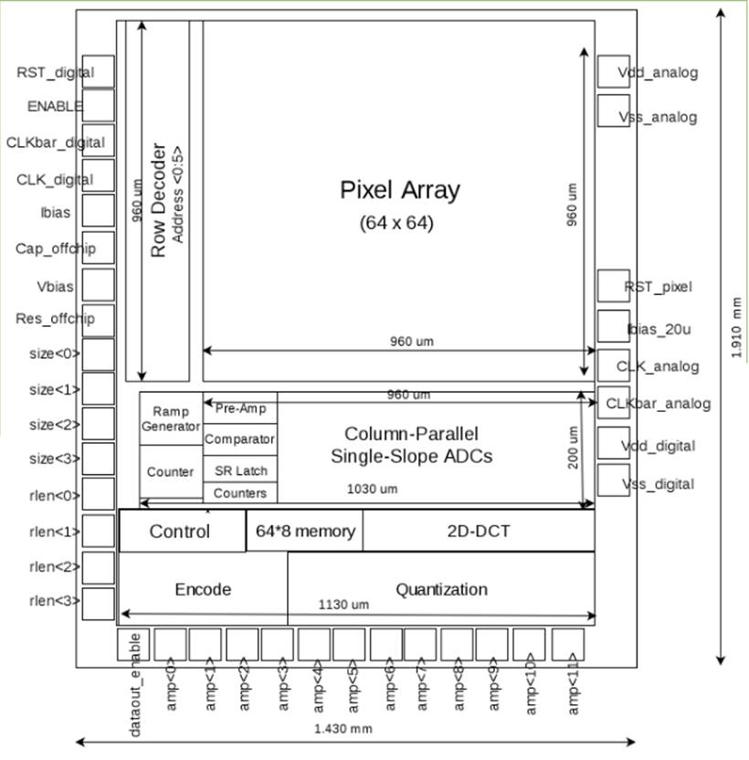
Figure 1. Floor plan of the whole chip
Analog Part
1. Row decoder
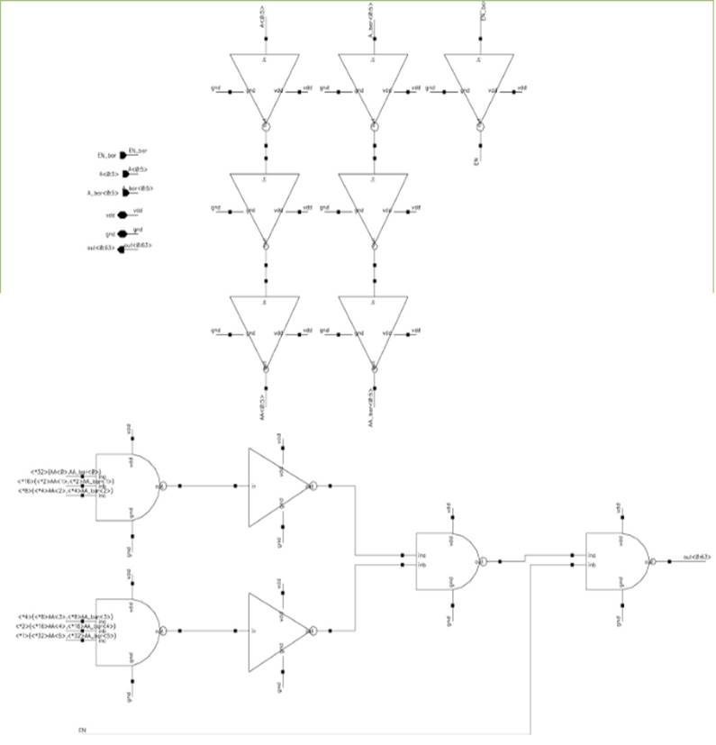
Figure 2. Schematic of row decoder
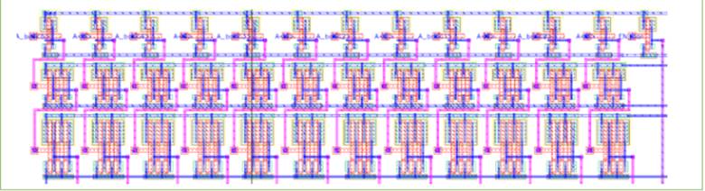
Figure 3. Layout of row decoder from stage 1 to stage 3 and enable inverter
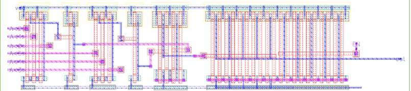
Figure 4. Layout of row decoder from stage 4 to stage 6 (1 out of 64 outputs)
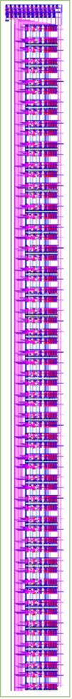
Figure 5. Layout of row decoder
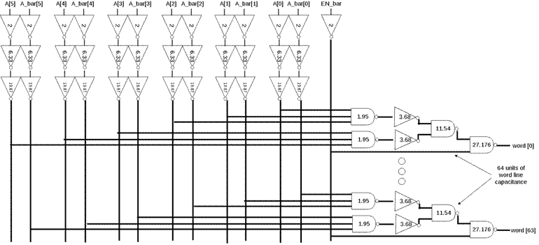
Figure 6. Block diagram and sizing of row decoder
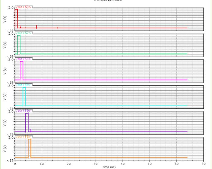
Figure 7. Part of simulation waveforms of row decoder outputs
2. RC ramp generator
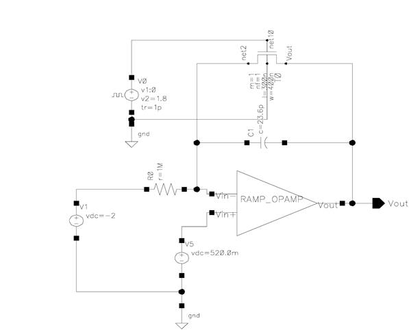
Figure 8. Testbench of RC ramp generator
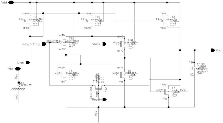
Figure 9. Schematic of RC ramp generator
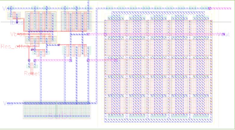
Figure 10. Layout of RC ramp generator
3. Column ADC schematic
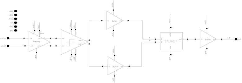
Figure 11. Schematic of column ADC in symbol view
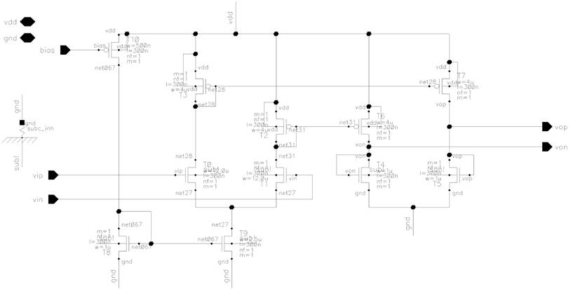
Figure 12. Schematic of preamplifier
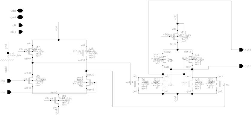
Figure 13. Schematic of latch comparator
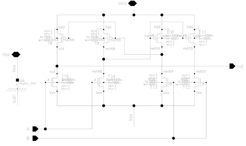
Figure 14. Schematic of SR latch
4. Column ADC Layout
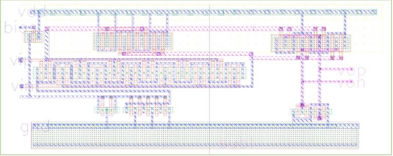
Figure 15. Layout of preamplifier
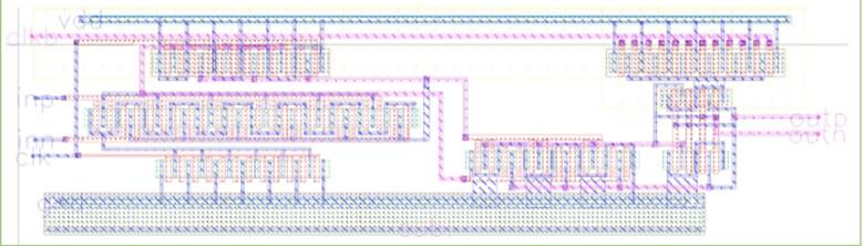
Figure 16. Layout of latch comparator
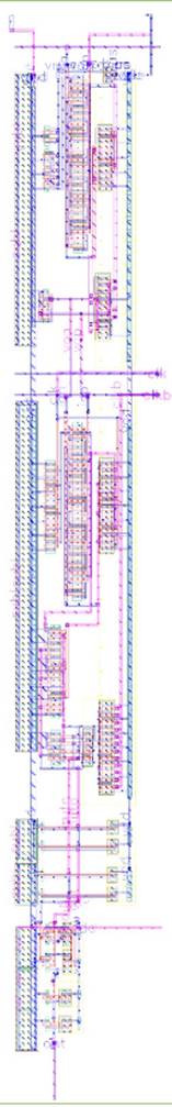
Figure 17. Layout of column ADC
5. Column-ADC simulation
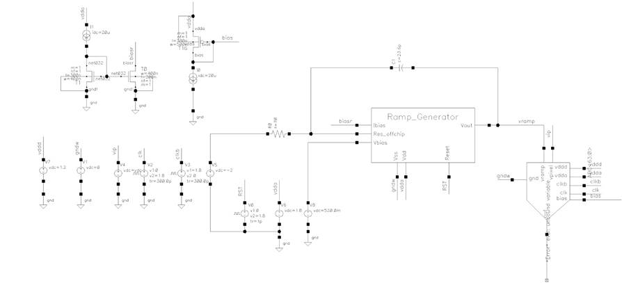
Figure 18. Test bench of column ADC
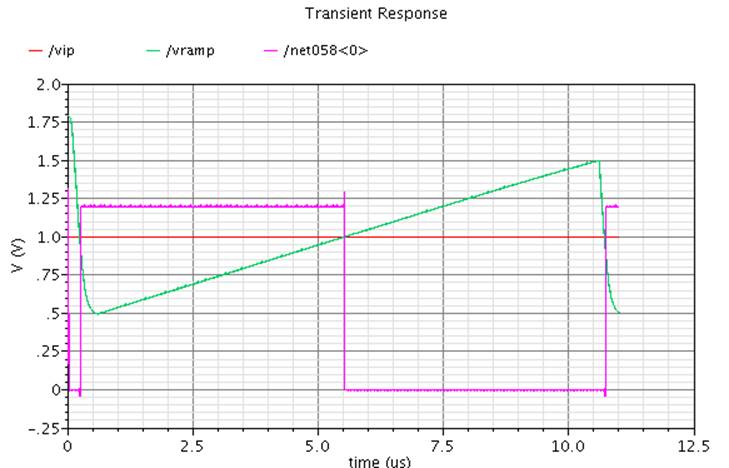
Figure 19. Simulation waveform of column ADC
Digital Part
1. Digital part
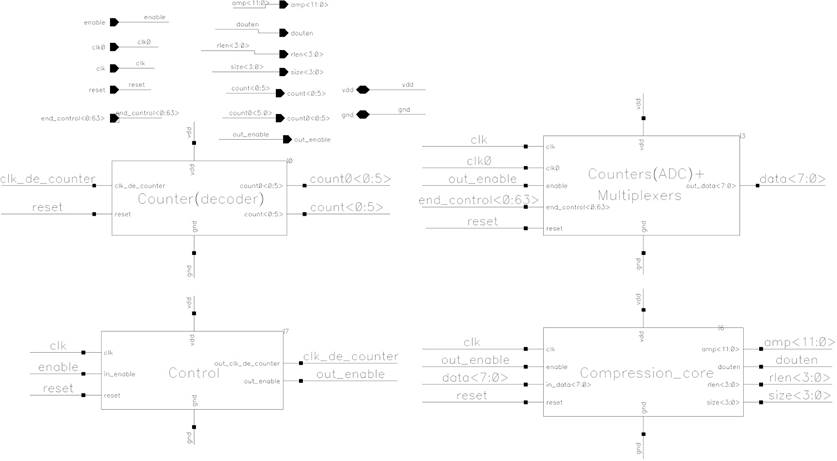
Figure 20. Schematic of digital part
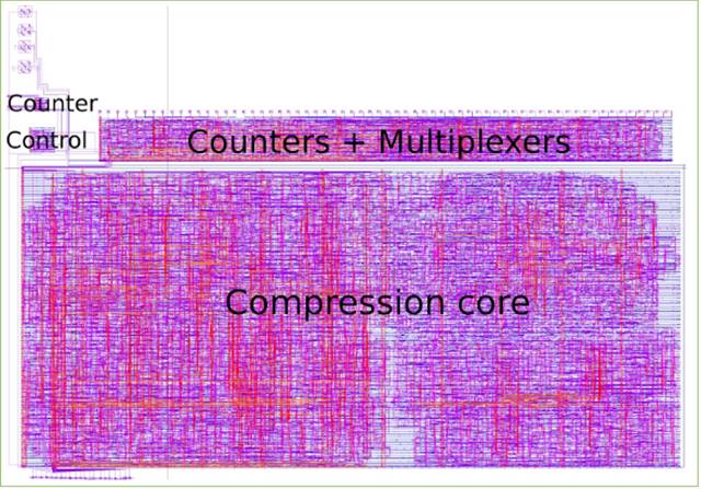
Figure 21. Layout of digital part
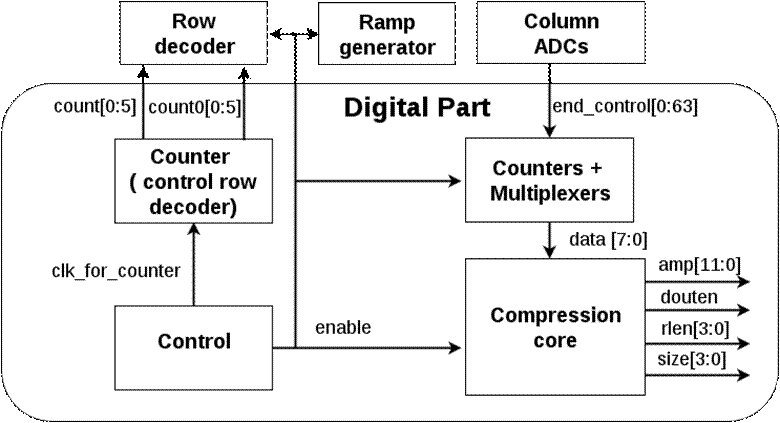
Figure 22. Block diagram of digital part
2. Compression core and its verification

Figure 23. Block diagram of compression core
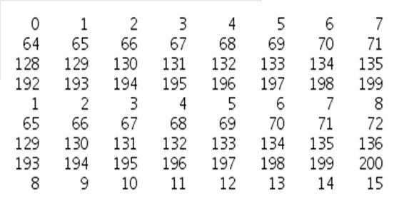
Figure 24. The 8*8 input matrix
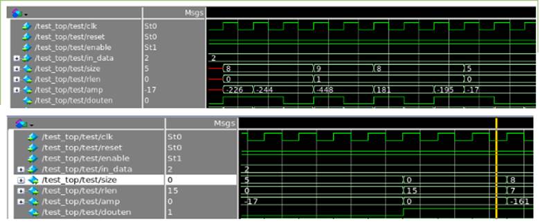
Figure 25. Output waveform in Modelsim

Figure 26. Output data of compression core
Organized in such format:
(Number of zeroes in front of the data (rlen[3:0]), data amplitude (amp[11:0]))

Figure 27. Output data of Matlab
Chip schematic and layout
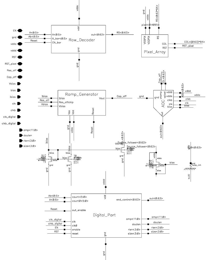
Figure 28. Schematic of entire chip
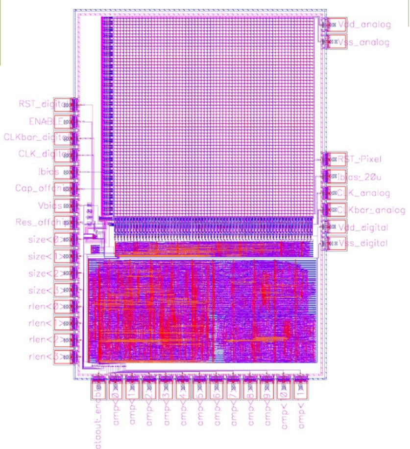
Figure 29. Layout of entire chip with padframe
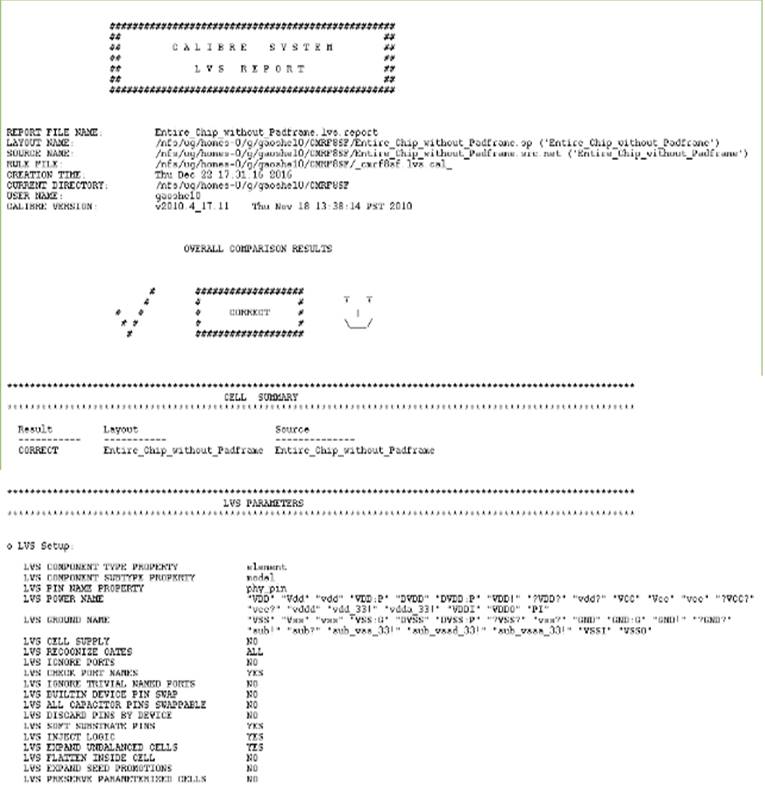
LVS
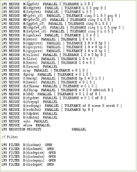
Instruction for running LVS and DRC:
Open the cell “Entire_chip_without_Padframe” in library “Finalproject_analog”
(LVS) Using the commands in LVS option:
LVS BOX LAYOUT digital_all
LVS BOX SOURCE digital_all
LAYOUT INPUT EXCEPTION SEVERITY MISSING_REFERENCE 1
(DRC) Using the commands in DRC option:
EXCLUDE CELL digital_all
LAYOUT INPUT EXCEPTION SEVERITY MISSING_REFERENCE 1
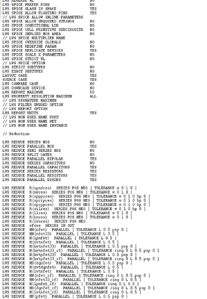
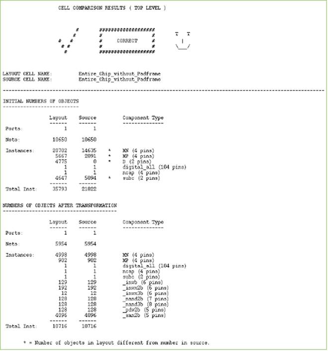
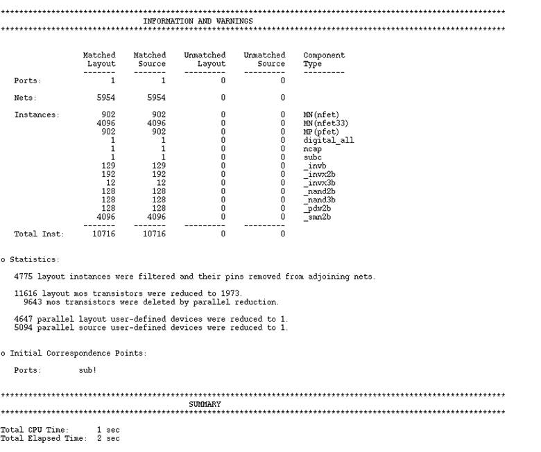
LVS Report:
References
[1] Cabeen, Ken, and Peter Gent. "Image compression and the discrete cosine transform." College of the Redwoods (1998).
[2] Ying Fang. “JPEG image compression based on FPGA.” pudn [Online]. Avaliable: http://www.pudn.com/downloads189/sourcecode/embed/detail889267.html [Accessed: Nov. 22, 2016]
[3] Schinkel, Daniel, et al. "A double-tail
latch-type voltage sense amplifier with 18ps setup+ hold time." 2007.